In this STM32 GPIO tutorial, we’ll discuss the STM32 GPIO hardware’s internal functionalities. How it works on low-level, so you can configure it in the best way to meet your applications’ needs. We’ll get into the GPIO speed, alternative functions, locking mechanism, and different possible configurations. So let’s get started!
Each of the general-purpose I/O ports has two 32-bit configuration registers, two 32-bit data registers, a 32-bit set/reset register, a 16-bit reset register, and a 32-bit locking register. Each I/O port bit is freely programmable, however, the I/O port registers must be accessed as 32-bit words (half-word or byte accesses are not allowed). The purpose of the set/reset registers is to allow atomic read/modify accesses to any of the GPIO registers. This way, there is no risk that an IRQ occurs between the read and modify access.
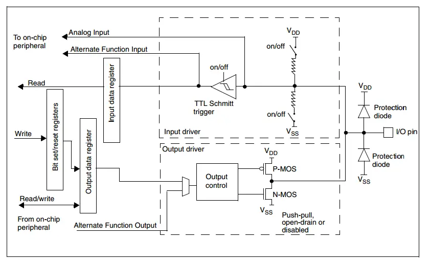
Here is a digital diagram for the internal structure of a typical GPIO pin. It shows the diode protection, internal pull-up or down enable/disable, and also the push-pull output driver, output enable/disable for switching between input/output pin modes, Schmitt-triggered digital input, and analog input.
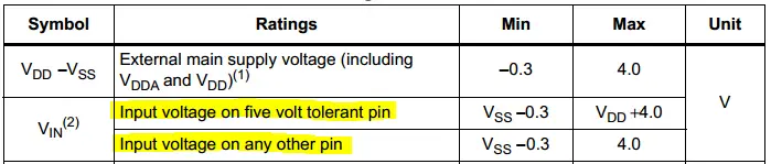
The STM32 GPIO output voltage level is 3.3v and the GPIO input voltage is also 3.3v while some of these input pins are 5v tolerant. But you have to refer to the datasheet to make sure which input pins are 5v tolerant.
You have to assume that all GPIO pins are not 5v tolerant by default until you find in the datasheet that a specific pin is 5v tolerant, only then you can use it as a 5v pin. The pins are mostly 3.3V and can be damaged when hooked up to 5V digital input lines. Level shifting may be mandatory in many cases.
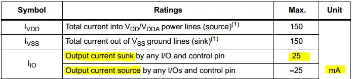
STM32 GPIO pins have a maximum current limit of 25mA per IO pin. This is the maximum current that can be sourced or sunk by any IO pin.
So you have to be careful with the voltage level for input pins. And also you’ve to pay attention to the output current when you set GPIO output pins. The maximum current that could be sourced or sunk into any GPIO pin is 25mA as per the datasheet. And you’ve to check it for the specific target STM32 microcontroller you’re dealing with.
The STM32 GPIO lines have a programmable speed control that can be used to set the “slew rate” of the IO lines which dictates the maximum allowable speed that the IO line can be driven at. In this section, we’ll summarize this GPIO speed control feature with all of its possible configurations (options).
When a GPIO pin is set to input mode, the data present on the I/O pin is sampled into the Input Data Register every APB2 clock cycle. This means the APB2 bus speed determines the input sampling speed for the GPIO pins.
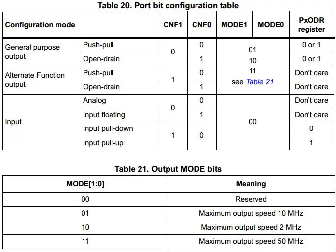
When a GPIO pin is set to output mode, you’ll have the option to configure the pin speed mode by programming the respective bits in the configuration registers. Down below is a table for the different modes available in the datasheet for the STM32F103C8 microcontroller.
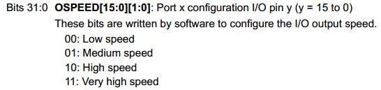
However, other microcontrollers will have different options for the pin output speed. For example, the other microcontroller we’ll be using in this course STM32L432KC. It has a dedicated speed control register for GPIO pins, which have 4 different speed options: Low-speed, Medium-speed, High-speed, and Very High-speed.
You’ll find what do these speed grades translate to in the device datasheet IO pin characteristics. Here is the table for this parameter from the STM32L432KC datasheet table.
Note: Typical values depend on various parameters of which the VDDio line voltage, and the total pin capacitance.
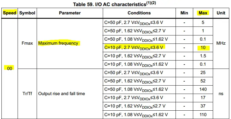 This table, for reference only, shows only the low-speed mode. The other modes are in the complete table in the datasheet.
There is no need for the software to disable interrupts when programming the GPIOx_ODR at the bit level: it is possible to modify only one or several bits in a single atomic APB2 write access. This is achieved by programming to ‘1’ the Bit Set/Reset Register (GPIOx_BSRR, or for reset only GPIOx_BRR) to select the bits to modify. The unselected bits will not be modified.
All ports have external interrupt capability. To use external interrupt lines, the port must be configured in input mode. We’ll discuss this in a more detailed manner when we get into the EXTI (external interrupt/event controller) topic.
To optimize the number of peripheral I/O functions for different device packages, it is possible to remap some alternate functions to some other pins. This is achieved by software, by programming the corresponding registers.
This option can help you remap the peripherals io pins, so you don’t have to change so much in the PCB layout when you change the target microcontroller on the board. This can be extremely advantageous and ease the routing process. And helps you move the high-speed signals away so as to reduce the noise level at certain parts.
The locking mechanism allows the IO configuration to be frozen. When the LOCK sequence has been applied to a port bit, it is no longer possible to modify the value of the port bit until the next reset.
Subject to the specific hardware characteristics of each I/O port listed in the datasheet, each port bit of the General Purpose IO (GPIO) Ports, can be individually configured by software in several modes:
Output Configuration
Input Configuration
Alternate Function Configuration
Analog Configuration
Not all STM32 GPIO Pin are 5v tolerant. Mostly they are 3.3v. You have to enable the clock for the GPIO you want to use regardless of the mode of operation. When configuring a GPIO output pin, you can select the speed suitable for your application whether you need high-frequency switching on the IO line or not.
The APB2 bus speed determines the sampling rate for all GPIO input configured pins. You can disconnect any GPIO pin (make it high impedance) by setting it into input mode with Hi-Z. You can freeze or lock the GPIO pins configuration after the system initialization if no change is intended using the locking mechanism.
Alternative function pins can be interchanged (remapped) internally so you can enjoy more freedom in routing these signals. All STM32 GPIO pins are interrupt-capable pins but have to be configured within the EXTI as we’ll see later on in this STM32 tutorials series.
Copyright ©2025. All Rights Reserved Emblab THE RAVE INNOVATION