This tutorial is the first part of our STM32 ADC Tutorial Series. In this tutorial series, you’ll learn everything about ADC in STM32 microcontrollers. We’ll go through examples for each and every single mode of operation (Single-Channel, Multi-Channel, Scan, Continuous Conversion, Discontinuous Mode, Injected Channels, Analog Watchdog, etc). We’ll perform the ADC data reading with all possible techniques for every mode of operation (using Polling, Interrupt, and DMA).
This pretty long journey starts off here, in this STM32 ADC Tutorial, where we’ll introduce all the fundamentals and the knowledge base that we’ll be using in later tutorials in this series. Without further ado, let’s get right into it!
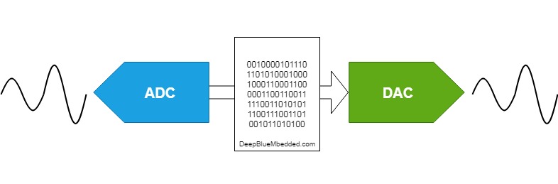
An ADC (Analog-To-Digital) converter is an electronic circuit that takes in an analog voltage as input and converts it into digital data, a value that represents the voltage level in binary code. The ADC samples the analog input whenever you trigger it to start conversion. It performs a process called quantization to decide on the voltage level and its binary code that gets pushed into the output register.
The ADC does the counter operation that of a DAC, while an ADC (A/D) converts analog voltage to digital data the DAC (D/A) converts digital numbers to the analog voltage on the output pin.
The ADC is one of the most expensive electronic components especially when it does have a high sampling rate and high resolution. Therefore, it’s a valuable resource in microcontrollers and different manufacturers provide us (the firmware engineers) with various features to make the best use of it. And the flexibility also to make a lot of decisions like sacrificing resolution in exchange for a higher resolution or having the ADC to trigger on an internal timer signal to periodically sample the analog channels, and much more as we’ll see in this tutorial.
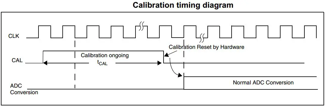
The ADC has a built-in self-calibration mode. Calibration significantly reduces accuracy errors due to internal capacitor bank variations. During calibration, an error correction code (digital word) is calculated for each capacitor, and during all subsequent conversions, the error contribution of each capacitor is removed using this code.
Calibration is started by setting the CAL bit in the ADC_CR2 register. Once calibration is over, the CAL bit is reset by hardware and normal conversion can be performed. It is recommended to calibrate the ADC once at power on. The calibration codes are stored in the ADC_DR as soon as the calibration phase ends. It is recommended to perform a calibration after each power-up.
The STM32 HAL does provide a function within the ADC APIs dedicated to starting the calibration process and as said before it’s a recommended step after initializing the ADC hardware at the system power-up.
The STM32 ADC samples the input voltage for a number of ADC_CLK cycles which can be modified using the SMP[2:0] bits in the ADC_SMPR1 and ADC_SMPR2 registers. Each channel can be sampled with different sample times.
The Total ADC Conversion Time is calculated as follows:
Tconv = Sampling time + 12.5 cycles
Example:
With an ADCCLK = 14 MHz and a sampling time of 1.5 cycles: Tconv = 1.5 + 12.5 = 14 cycles = 1 µs
The ADC Sampling Rate (Frequency) is calculated using this formula:
SamplingRate = 1 / Tconv
For The Previous example where Tconv = 1µs, The samplingRate = 1000000 = 1Ms/sec
The STM32 ADC has a resolution of 12-bit which results in a total conversion time of SamplingTime+12.5 clock cycles. However, higher sampling rates can be achieved by sacrificing the high resolution. Therefore, the resolution can be dropped down to 10-bit, 8-bit, or 6-bit, and hence the conversion time is much shorter, and the sampling rate increases.
This can be configured and implemented in software by the programmer and the STM32 HAL does provide APIs to set all the ADC parameters including its resolution.
The ADC reference voltage pins are defined in the datasheet and assumed to be connected to a voltage level in a certain range. This is shown in the table below. You can choose to set the reference voltage to its maximum allowable level for a wider range of conversion but less voltage measurement resolution. Alternatively, you can set the reference voltage to the minimum allowable value for better voltage reading resolution.
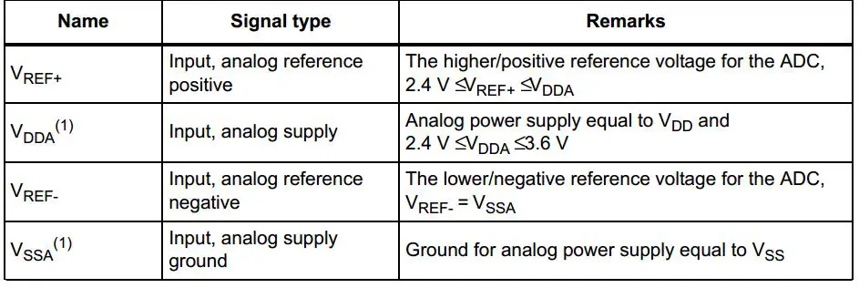
If you’re using a development board, you may need to check out its schematic diagram as it may not be connecting the ADC Vref at all or connecting it to a 2.5v for example, so the ADC will saturate and give you 4096 before the input analog voltage reaches 3.3v and you’re wondering why! it may be because the reference voltage is set to a value less than 3.3v, so it’s something to consider.
ADC Conversion Time
Tconv = Sampling time + 12.5 cycles
ADC Sampling Rate
SamplingRate = 1 / Tconv
ADC Result Voltage (Analog Input Value)
Vin = ADC_Res x (Reference Voltage / 4096)
Where, Reference Voltage = (VREF+) – (VREF-)
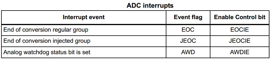
An interrupt can be produced at the end of conversion for regular and injected groups and when the analog watchdog status bit is set. Separate interrupt enable bits are available for flexibility.
Since converted regular channel values are stored in a unique data register, it is necessary to use DMA for the conversion of more than one regular channel. This avoids the loss of data already stored in the ADC_DR register.
Only the end of the conversion of a regular channel generates a DMA request, which allows the transfer of its converted data from the ADC_DR register to the destination location selected by the user.
There are mainly three different ways to read the STM32 ADC conversion result upon conversion completion. In this section, we’ll briefly describe each method and in the following tutorials, we’ll implement all of those 3 techniques for each operation mode of the ADC.
It’s the easiest way in code to perform an analog-to-digital conversion using the ADC on an analog input channel. However, it’s not an efficient way in all cases as it’s considered to be a blocking way of using the ADC. Because in this way we start the A/D conversion and wait for the ADC until it completes the conversion so the CPU can resume processing the main code.
The interrupt method is an efficient way to do ADC conversion in a non-blocking manner, so the CPU can resume executing the main code routine until the ADC completes the conversion and fires an interrupt signal so the CPU can switch to the ISR context and save the conversion results for further processing.
However, when you’re dealing with multiple channels in a circular mode or so, you’ll have periodic interrupts from the ADC that are too much for the CPU to handle. This will introduce jitter injection, interrupt latency, and all sorts of timing issues to the system. This can be avoided by using DMA.
Lastly, the DMA method is the most efficient way of converting multiple ADC channels at very high rates and still transfers the results to the memory without CPU intervention which is so cool and time-saving technique.
Note That: Code Examples For The 3 Methods Are Provided in The Next Tutorials.
The next section will help you identify and optimize the error sources in your STM32 ADC measurement system. However, it’s not mandatory for everyone to study it in the meantime and you can now move on to the next part of this STM32 ADC tutorial series.
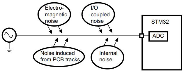
This section lists the main error types that have an effect on A/D conversion accuracy. These types of errors occur in all A/D converters and conversion quality depends on eliminating the source of each error of them.
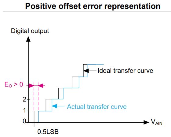
1.1 – ADC Offset Error
The offset error is the deviation between the first actual transition and the first ideal transition. The first transition occurs when the digital ADC output changes from 0 to 1. Ideally, when the analog input ranges between 0.5 LSB and 1.5 LSB, the digital output should be 1. Still, ideally, the first transition occurs at 0.5 LSB. The offset error is denoted by EO. The offset error can easily be calibrated by the application firmware.
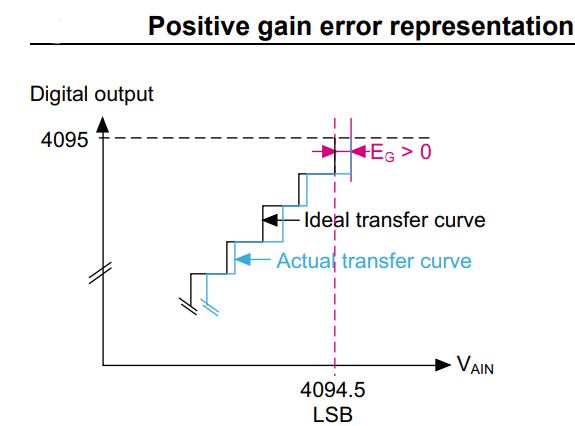
1.2- ADC Gain Error
The gain error is the deviation between the last actual transition and the last ideal transition. It is denoted by EG. The last actual transition is the transition from 0xFFE to 0xFFF. Ideally, there should be a transition from 0xFFE to 0xFFF when the analog input is equal to VREF+ – 0.5 LSB. So for VREF+= 3.3 V, the last ideal transition should occur at 3.299597 V. If the ADC provides the 0xFFF reading for VAIN < VREF+ – 0.5 LSB, then a negative gain error is obtained. The gain error is obtained by the formula below:
EG = Last actual transition – ideal transition
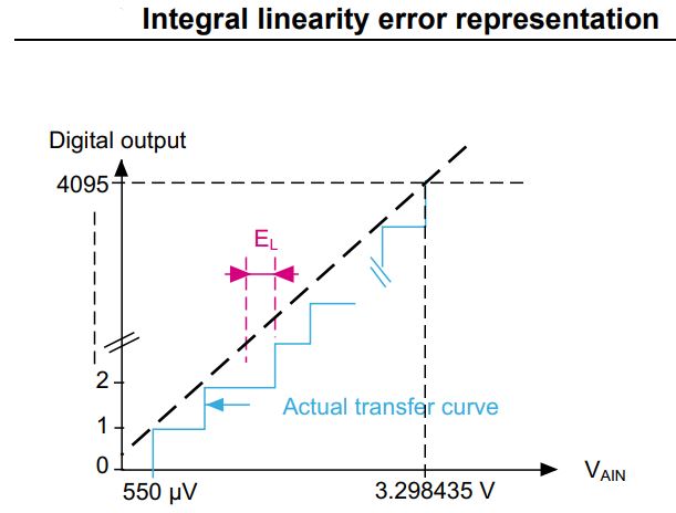
1.3 – Integral Linearity Error
The integral linearity error is the maximum deviation between any actual transition and the endpoint correlation line. The ILE is denoted by EL. The endpoint correlation line can be defined as the line on the A/D transfer curve that connects the first actual transition with the last actual transition.
EL is the deviation from this line for each transition. The endpoint correlation line thus corresponds to the actual transfer curve and has no relation to the ideal transfer curve. The ILE is also known as the integral non-linearity error (INL). The ILE is the integral of the DLE over the whole range.
2.1 – ADC Reference Voltage Noise
As the ADC output is the ratio between the analog signal voltage and the reference voltage, any noise on the analog reference causes a change in the converted digital value. VDDA analog power supply is used on some packages as the reference voltage (VREF+), so the quality of the VDDA power supply has an influence on ADC error.
2.2 – Analog Input Signal Noise
Small but high-frequency signal variation can result in big conversion errors during sampling time. This noise is generated by electrical devices, such as motors, engine ignition, power lines. It affects the source signal (such as sensors) by adding an unwanted signal. As a consequence, the ADC conversion results are not accurate.
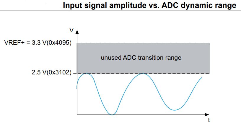
2.3 – ADC Dynamic Range Bad Matching
To obtain the maximum ADC conversion precision, it is very important that the ADC dynamic range matches the maximum amplitude of the signal to be converted. Let us assume that the signal to be converted varies between 0 V and 2.5 V and that VREF+ is equal to 3.3 V. The maximum signal value converted by the ADC is 3102 (2.5 V) as shown in the diagram down below. In this case, there are 993 unused transitions (4095 – 3102 = 993). This implies a loss in the converted signal accuracy.
2.4 – Analog Signal Source Impedance (Resistance)
The impedance of the analog signal source, or series resistance (RAIN), between the source and pin, causes a voltage drop across it because of the current flowing into the pin. The charging of the internal sampling capacitor (CADC) is controlled by switches with a resistance RADC. With the addition of source resistance (with RADC), the time required to fully charge the hold capacitor increases.
If the sampling time is less than the time required to fully charge the CADC through RADC + RAIN (ts < tc), the digital value converted by the ADC is less than the actual value.
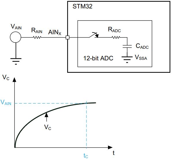
This error can be reduced or completely eliminated by setting the sampling time of the analog channel in such a way that guarantees an appropriate voltage level on the input pin is present before the ADC starts the conversion.
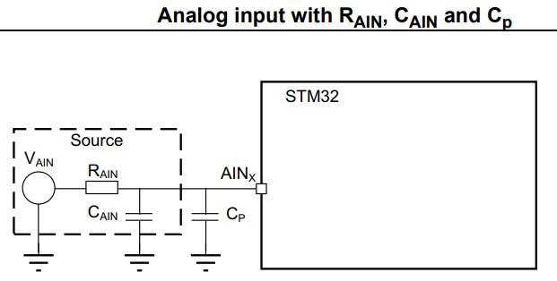
2.5 – Analog Signal Source Capacitance & Parasitics
When converting analog signals, it is necessary to account for the capacitance at the source and the parasitic capacitance seen on the analog input pin. The source resistance and capacitance form an RC network. In addition, the ADC conversion results may not be accurate unless the external capacitor (CAIN + Cp) is fully charged to the level of the input voltage.
The greater value of (CAIN + Cp), the more limited the source frequency. The external capacitance at the source and the parasitic capacitance are denoted by CAIN and Cp, respectively.
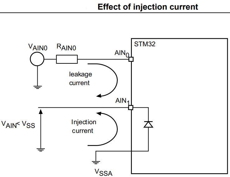
2.6 – Injection Current Effect
A negative injection current on any analog pin (or a closely positioned digital input pin) may introduce leakage current into the ADC input. The worst case is the adjacent analog channel. A negative injection current is introduced when VAIN < VSS, causing current to flow out from the I/O pin. Which can potentially shift the voltage level on the pin and distort the measurement result.
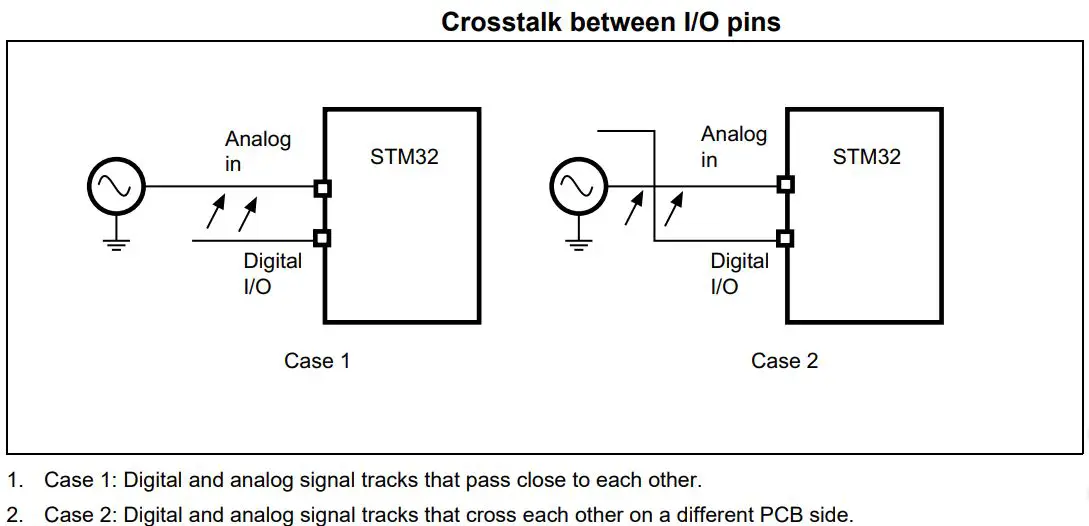
2.7 – IO Pins Cross-Talking
Switching the I/Os may induce some noise in the analog input of the ADC due to capacitive coupling between I/Os. Crosstalk may be introduced by PCB tracks that run close to each other or that cross each other.
Internally switching digital signals and IOs introduces high-frequency noise. Switching high sink I/Os may induce some voltage dips in the power supply caused by current surges. A digital track that crosses an analog input track on the PCB may affect the analog signal.
2.8 – EMI-Induced Noise
Electromagnetic emissions from neighboring circuits may introduce high-frequency noise in an analog signal because the PCB tracks may act as an antenna. It’s called electromagnetic interference (EMI) noise.
In the next few tutorials, we’ll be practicing the ADC peripheral and doing some practical LABs to learn how to configure and program the ADC to do certain tasks in different ways. The ADC example applications will include the following:
Copyright ©2025. All Rights Reserved Emblab THE RAVE INNOVATION